


Tata Electronics: How Is ASML Helping Build Semiconductors in India?
Synopsis: Tata Electronics’ partnership with ASML marks a major step in India’s semiconductor ambitions. By bringing advanced lithography technology, 300 mm wafer manufacturing, talent development and supply chain capabilities to the Dholera fab, the collaboration aims to position India as a serious semiconductor manufacturing and AI infrastructure player. India’s semiconductor ambitions gained fresh momentum after Tata […] The post Tata Electronics: How Is ASML Helping Build Semiconductors in India? appeared first on Trade Brains.

Synopsis: Tata Electronics’ partnership with ASML marks a major step in India’s semiconductor ambitions. By bringing advanced lithography technology, 300 mm wafer manufacturing, talent development and supply chain capabilities to the Dholera fab, the collaboration aims to position India as a serious semiconductor manufacturing and AI infrastructure player.
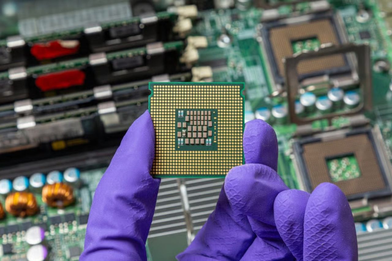
India’s semiconductor ambitions gained fresh momentum after Tata Electronics signed a strategic partnership with ASML, one of the world’s leading semiconductor equipment companies. The collaboration will support the development of Tata Electronics’ upcoming 300 mm semiconductor fabrication plant in Dholera, Gujarat.
Beyond manufacturing, the agreement focuses on lithography technology, research infrastructure, talent development and supply chain resilience. As countries worldwide compete for semiconductor leadership, this partnership signals India’s growing intent to become a global semiconductor manufacturing and AI infrastructure hub.
India’s Semiconductor Push Gets a Global Technology Partner
The semiconductor segment in India has taken its next step as Tata Electronics partnered with ASML in a move that could change how semiconductors are made in India. The signing of the MOU between the two companies is a crucial milestone in India’s endeavour to position itself as a semiconductor manufacturing destination. As part of the pact, ASML will assist Tata Electronics in setting up and scaling operations for its next-generation 300 mm semiconductor wafer fab plant in Dholera, Gujarat.
This strategic alliance comes amid attempts by many nations to diversify their semiconductor supply chains and lessen reliance on select manufacturing sites. In fact, this is much more than just a simple manufacturing plant that India is trying to set up with this deal. It represents an effort made by India to become part of one of the most advanced sectors of the world.
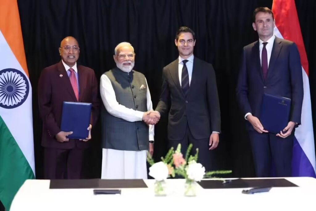
India-Netherlands ties have shown increasing signs of progress in recent times, and this agreement is further testimony to the rising levels of technology cooperation between the two countries in the semiconductor industry and others. According to the Tata Electronics statement, ASML will provide its latest lithography technologies and operational capabilities at the Indian semiconductor fab plant.
Why the Dholera Fab Is a Landmark Project
The Dholera semiconductor fabrication unit is arguably one of the most ambitious manufacturing units in technology production in the country. Tata Electronics is setting up the first-ever commercial 300 mm semiconductor fabrication unit in India that will cost about US$11 billion. The fab plant will produce chips meant for various advanced technology products, like use in automobiles, phones, artificial intelligence systems and many more.
It is a highly strategic move due to the reasons that semiconductor fabrication has always been dominated by a select number of countries, which are Taiwan, South Korea and the US. Although India has had semiconductor design and software services before, it lacks the capability to conduct large-scale front-end semiconductor manufacturing. This is where the Dholera project comes in.
Already, Tata Electronics has made partnerships with Taiwan-based Powerchip Semiconductor Manufacturing Corporation, known popularly as PSMC, giving it the ability to leverage technology ranging from 28 nm, 40 nm, 55 nm, 90 nm and 110 nm process technologies. In addition, the collaboration with ASML brings in one of the most critical players in semiconductors into the ecosystem.
Understanding the Importance of 300 mm Wafers
One of the critical components of the Dholera fab involves 300 mm semiconductor wafers, which are the global industrial benchmark for semiconductor-manufacturing processes. A wafer refers to a thin silicon disc that is used in the fabrication of microchips and other integrated circuits.
The advantage of 300 mm wafers in manufacturing lies in their efficiencies. Large-sized wafers enable semiconductor companies to produce more chips within the same manufacturing cycle, making processes economical due to improved manufacturing economies of scale. In addition, a majority of chips found in AI servers, data centres, smartphones, and next-generation automobiles utilise 300 mm wafers.
Semiconductor manufacturing processes are based on two main stages that include wafer fabrication during front-end processes and packaging and testing during back-end processes. As such, wafer fabrication constitutes the core of semiconductor manufacturing processes. The establishment of a commercial-scale 300 mm fab marks an effort by India to create capabilities in one of the most technically challenging areas of the semiconductor value chain.
Therefore, the Dholera fab is not just a manufacturing plant but represents an effort by India to create semiconductor infrastructure in view of future technological development across industries like AI and advanced mobility.
How ASML’s Lithography Technology Fits Into the Project
It is especially important because lithography is considered one of the crucial steps in semiconductor production since the lithography system serves to project tiny circuit patterns onto silicon wafers for chip-making.
ASML is well known all around the world as one of the major producers of semiconductor equipment, providing chipmakers with necessary hardware, software, and service for the mass production of integrated circuits. Its technologies are widely used for modern semiconductor manufacturing all over the world.
As per the contract, ASML will use its “holistic suite” of lithography equipment for the Dholera fab. As stated by Tata Electronics, this cooperation will enable timely ramp-up of the facility with high-quality standards of manufacturing and operation.
Another aspect of cooperation between the companies includes R&D infrastructure, which needs to be built for successful long-term operation of the first-ever commercial fab in India. It is especially important because semiconductor production implies constant optimisation of processes and updating equipment due to continuous improvement of manufacturing techniques and technologies. For Tata Electronics, the agreement will contribute to the strengthening of the company’s relations within the entire semiconductor value chain.
Building Talent and Supply Chain Capabilities in India
One of the most crucial parts of the deal is the emphasis on talent development and ecosystem creation. The process of fabrication of semiconductors is highly specialised and requires specialists skilled in lithography, process integration, materials engineering and yield optimisation.
The companies behind the project plan to work together in order to implement talent development projects, training and educational programmes and research initiatives in order to create a local talent pool. This collaboration will help accelerate development of lithography-related skills and ensure that there are a sufficient number of professionals who could operate an advanced semiconductor fab.
This is especially important due to the fact that India is well known in the field of semiconductor design and engineering services, and the country possesses about 20 per cent of all chip designers in the world. It seems that currently the Indian government, as well as the companies operating in the sector, are trying to take advantage of the existing pool of talented professionals.
Tata Electronics has been collaborating with a number of Indian and international institutions in order to train local professionals in semiconductor manufacturing. The cooperation with ASML might help them do that more efficiently.
The agreement also seeks to create a more resilient semiconductor supply chain within India. Semiconductor manufacturing relies on a large ecosystem of equipment suppliers, chemical providers, specialty gas manufacturers and precision engineering firms. Building these supply chains locally is essential for long-term sustainability.
Why the Deal Matters Strategically for India
The significance of the Tata-ASML partnership is being perceived in the light of the increasing importance of semiconductors in the spheres of economic competitiveness, national security and even AI supremacy. The analysts interviewed in the transcript mentioned the pact as one of the most important events related to semiconductors to occur in India recently.
The signing of this pact shows how India is looking to shift from its reputation as a supplier of software services and engineering professionals to being an active participant in the development of the physical infrastructure required for the functioning of the AI industry. High-end chips are necessary for the operation of AI servers, clouds and other devices.
It should also be highlighted that this event is connected with the strategy of making India one of the leaders of the AI industry by creating a robust digital infrastructure. In 2024, the India AI Mission was launched with the aim of allocating $1.07 billion for investments into computing infrastructure, research work, and assistance to startups.
As emphasized by the experts interviewed in the transcript, semiconductor production is crucial for maintaining technological independence. All countries seek access to semiconductors now, having realised the dangers of dependence on the global semiconductor market.
India’s Semiconductor Journey Still Faces Challenges
While there is certainly hope for the partnership between Tata and ASML, India still continues to face many challenges in terms of achieving their goal to create a semiconductor industry. The semiconductor industry is probably one of the most technologically advanced and capital-intensive industries worldwide.
The fact that the semiconductor industry has been unsuccessful in its previous projects has shown that the Indian government needs to work harder on its semiconductor plans. For example, Foxconn backed out of the plan to build a semiconductor joint venture with the Vedanta conglomerate due to delays in government incentive approvals in 2023.
Another important point regarding the semiconductor industry is that the equipment and components used can often be sourced from other countries. This means that developing a semiconductor ecosystem in India will take time because it is hard to isolate the industry from other countries.
In this regard, Tata and ASML’s collaboration seems much more focused on creating an ecosystem and technology rather than building a semiconductor industry within a year. Another positive thing about the project is the participation of global semiconductor companies such as ASML and PSMC.
A Defining Moment for India’s Semiconductor Ambitions
The partnership between Tata Electronics and ASML might be considered among the pivotal developments for India’s semiconductor story. Given the combination of manufacturing capabilities provided by Tata Electronics with the lithography solutions offered by ASML, the cooperation seeks to build India’s first semiconductor production ecosystem based on the 300 mm wafer process.
Notably, it is important not just to have a semiconductor plant built but also the entire ecosystem developed around it, including manufacturing technologies, talent pool development, supply chain reinforcement, and R&D efforts infrastructure, which are all indispensable elements of any sustainable semiconductor industry.
It should be mentioned that India’s aspirations regarding its development into the global semiconductor and AI infrastructure powerhouses are yet to reach maturity and face some practical difficulties in implementation. Nevertheless, with its cooperation with ASML, India seems to start shifting from its traditional role as the main supplier of software talent to one of a manufacturing player.
For Tata Electronics, the partnership positions the company at the centre of India’s semiconductor manufacturing ambitions. For ASML, it opens a new long-term growth opportunity in one of the world’s fastest-growing technology markets. And for India, the collaboration represents an important step toward building domestic semiconductor capability in an industry that is increasingly shaping the future of global technology and economic power.
Disclaimer: The views and investment tips expressed by investment experts/broking houses/rating agencies on tradebrains.in are their own, and not that of the website or its management. Investing in equities poses a risk of financial losses. Investors must therefore exercise due caution while investing or trading in stocks. Trade Brains Technologies Private Limited or the author are not liable for any losses caused as a result of the decision based on this article. Please consult your investment advisor before investing.
The post Tata Electronics: How Is ASML Helping Build Semiconductors in India? appeared first on Trade Brains.
What's Your Reaction?